
PMOS and NMOS symbols, two of the basic MOSFET (Metal Oxide Semiconductor Field Effect Transistor) devices, are two of the most important symbols in semiconductor and transistor-based design. Symbols are the vocabulary of electronics. Symbols reduce complex circuits into understandable schematics. They are the foundation of digital electronics, microprocessors, and integrated circuits powering our everyday devices.
NMOS and PMOS are the opposites of the same thing, one works at low voltage while the other at high voltage. They together form the brain of CMOS (Complementary Metal Oxide Semiconductor) technology, which is the backbone of almost all of today’s digital devices.
Here, in this article, the author is talking about what PMOS and NMOS symbols are, how they differ from each other, how they are used in circuits, and what their importance is in the modern world of electronics.
Understanding the PMOS and NMOS Definition
Both PMOS and NMOS are MOSFETs, which are voltage-controlled current transistors.
- PMOS (P-type MOSFET) is ON when the gate voltage is negative (with respect to the source).
- NMOS (N-type MOSFET) is ON when there is a high gate voltage (relative to the source).
Both are employed in signal generation or amplification of electronic signals. Both are binary and digital logic ON/OFF switches.
In particular:
- NMOS is ON when gate voltage is present.
- PMOS is OFF when gate voltage is present.
They act as complements of each other precisely and work optimally when they are combined in CMOS design.
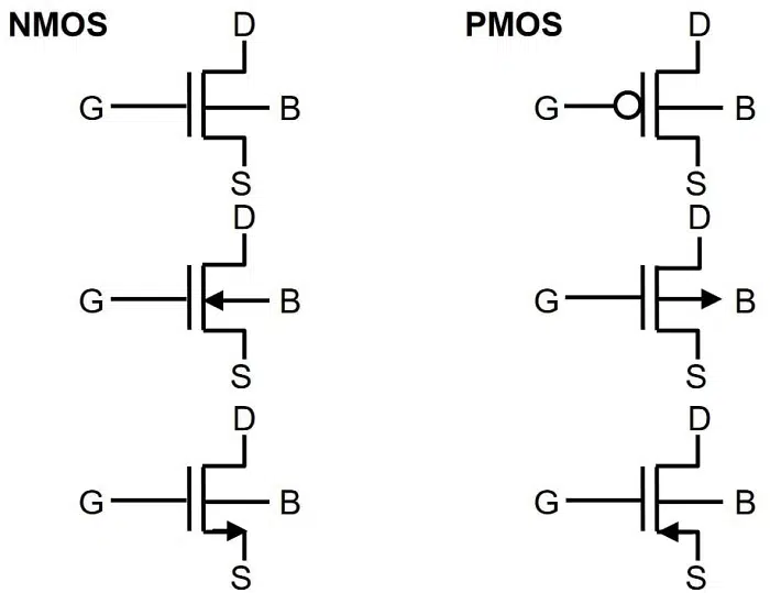
Symbol of NMOS and PMOS
NMOS and PMOS transistor symbols are alike but vary from each other in very significant manners, both in diagram and direction of current flow through them.
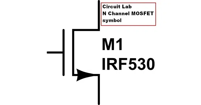
NMOS Symbol
NMOS symbol consists of three terminals:
- Drain (D) – Output current
- Gate (G) – Input voltage control
- Source (S) – Input current
In the NMOS symbol, the source arrow direction is outwards, indicating the electrons move from source to drain. The transistor conducts if a positive gate voltage is applied.
| Terminal | Symbol | Function |
| Gate (G) | Vertical line | Controls current flow |
| Drain (D) | Top line | Output for current |
| Source (S) | Bottom line with arrow pointing out | Presentation of electrons (shows N-type) |
It is the most common symbol utilized in amplifier circuit diagrams, logic gate circuit diagrams, and IC circuit diagrams.
PMOS Symbol
The PMOS symbol also consists of three terminals:
- Drain (D) – Current exit
- Gate (G) – Voltage input
- Source (S) – Current entry
In the PMOS symbol, the source arrow is pointed inward. Because holes (positive charge carriers) move from source to drain. The transistor is activated when the gate voltage is low.
| Terminal | Symbol | Function |
| Gate (G) | Vertical line | Switches flow of holes on and off |
| Drain (D) | Top line | Current exit |
| Source (S) | Bottom line with arrow pointing in | Holes’ entry (denotes P-type) |
The direction of the arrow change, thus, is the most important method of PMOS and NMOS identification from a schematic circuit.
PMOS and NMOS Operation
NMOS Working Principle:
A positive gate voltage repels electrons towards the channel. Which creates a path for current between drain and source. The current flows with no restriction, and the transistor is ON.
When no voltage is applied to the gate, the transistor is OFF and the channel is insulating.
PMOS Working Principle:
If a negative voltage (or a low voltage relative to the source) is applied to the gate. Then current is permitted to flow. If the gate voltage is high. Then the transistor is OFF and the channel is closed.
So, NMOS and PMOS are functioning oppositely.
| Type | Conducts When | Channel Type | Carrier Type |
| NMOS | Gate voltage is HIGH | N-type | Electrons |
| PMOS | Gate voltage is LOW | P-type | Holes |
CMOS – Composite of PMOS and NMOS
PMOS and NMOS are integrated in circuits as CMOS (Complementary MOS) logic. Both transistors are utilized in a pair with one in the on state and the other in the off state.
It offers:
- Efficiency with low power usage
- High-speed switching for better performance in digital circuits
- Reliability with low voltage drop and heat generation
CMOS technology is used in:
- Microprocessors and microcontrollers
- Memory chips (RAM, ROM)
- Digital watches
- Smartphones and cameras
In an NMOS transistor, the output is pulled low when the input is high. And in a PMOS, the output is pulled high when the input is low. This is the principle of binary logic (1 and 0).
The Circuit Symbol and Layout
PMOS and NMOS are both shown together in a complementary layout in a circuit diagram.
Example CMOS Inverter Circuit:
Vdd —|> PMOS
|
+—- Output
|
|> NMOS
Ground —-
PMOS is connected with supply (Vdd).
NMOS is connected with ground.
Output is taken between them.
At high input, NMOS is ON and pulls output low.
At low input, PMOS is ON and pulls output high.
Applications of PMOS and NMOS
PMOS and NMOS have wide applications in digital and analog electronics.
Applications of NMOS:
- Digital logic circuits
- Amplifiers
- Switching regulators
- Level shifters
- Motor controllers
Applications of PMOS:
- High-side switches
- Load drivers
- Analog filters
- Pull-up circuits
- Complementary logic with NMOS
They form ultra-low power logic gates used in billions of transistors per chip in today’s processors when paired together in CMOS circuits.
How to Identify PMOS and NMOS on Diagrams
In circuit schematic or IC design, it is easy to tell if a MOSFET is NMOS or PMOS using these clues:
| Feature | NMOS | PMOS |
| Arrow Direction | Outward | Inner |
| Substrate Type | P-substrate | N-substrate |
| Turn-On Voltage | Positive | Negative (or zero) |
| Symbol Placement | Bottom side of CMOS pair | Top side of CMOS pair |
| Common Use | Ground switching | Power supply switching |
PMOS and NMOS History
MOS technology began in the 1960s. Transistors were extremely large and power-hungry in those days. Mohamed Atalla and Dawon Kahng created the MOSFET (Metal-Oxide-Semiconductor Field-Effect Transistor) in 1959 and changed everything.
PMOS transistors arrived first in the 1960s and entered the microchips early.
NMOS transistors arrived next, with improved switching speeds.
Engineers in the 1970s wedded the two in CMOS technology, and it dramatically reduced power consumption and led the way to today’s computer revolution.
There are billions of PMOS and NMOS transistors in every microchip today that operate behind the scenes to compute the information driving our world.
Also Read: First Angle Projection Symbol: Definition, Origin, Use, and Importance in Engineering Drawing
What PMOS and NMOS Symbols Mean in Electronic Circuit Design
PMOS and NMOS symbols aren’t doodles. They’re deliberate.
They do:
- Differentiate among various transistors on schematic diagrams
- Determine the direction of signal flow
- Minimize logic circuits
- Describe circuit design principles globally without any language barrier
A circuit can be just looked at by a designer and determine how it functions according to the direction of the arrow in MOSFET’s symbol.
The Psychology of Visual Symbols in Engineering
PMOS and NMOS are notionally technical, indeed, but graphical formulations in which abstract concepts are made concrete. Geometric shapes are more congenial to engineers than words, bare use of an arrow or line shape conjures up reason, activity, and direction of current in one stroke.
In learning, the use of symbols aids visual memory. In professional design, they form an exact vocabulary and international cooperation.
Why PMOS and NMOS Are the Foundation of Electronics
All modern microchips, computers, and cell phones operate based on the principles of these two families of transistors. Their complementary opposite function allows for:
- Logical processing
- Efficient switching
- Stable voltage level operation
- Miniatured chip design
If electricity is the lifeblood of technology. Then PMOS and NMOS are its pulse.
PMOS and NMOS symbols write the double meaning of electronic logic, positive and negative, on and off, true and false. Their form shapes the design arts of modern electronic design and computation.
From the first applications of silicon wafers to the latest high-tech 5-nanometer chips, PMOS and NMOS transistors and their Spartan symbols have allowed engineers to construct the digital world.
Those lines, arrows, and symbols are all signs of flow, control, and precision that continue to energize the devices in our pockets, beds, and elsewhere.